Dumping firmware from a router
A couple of months ago I upgraded my DSL line and my ISP was kind enough to provide me with a new modem. To my surprise the interface was pretty locked down compared to my previous one, so a question came into my mind; is there a super admin password that could unlock the interface? But where is the firmware to analyze? My provider stopped publicly sharing the latest firmware and the published ones are encrypted . I decided to mess with my older router and try to dump the firmware.
Locating the flash chip
After opening the device I tried to find the flash chip. Usually, flash chips are located near the CPU (in the next photo, under the big grilled heatsink). The flash chip was a Macronix NAND chip.

The first obstacle appeared very early on this project. All the guides and writeups I read about flash dumping were based on two components. Firstly the chip was usually a NOR chip and dumped by the Flashrom tool https://www.flashrom.org/Flashrom. However, Flashrom does not support NAND chips. Secondly and most importantly the packaging of the chip is a WSON-8. What does this mean? The pins are not accessible and they are hidden underneath the chip. Most articles were discussing about an SOP-8 package were the pins were accessible and special hooks could be used to probe the flash chip.

Hardware for desoldering
The only way to overcome this problem is unfortunately to desolder the flash chip. For someone like me with no experience or knowledge in hardware or electronics that seemed an impossible task guaranteed to fail. I hadn’t even touched a soldering iron before. It happens that I follow a Youtube channel called NorthridgeFix https://www.youtube.com/@NorthridgeFix so I had a basic idea of how such things could work for me. Some hardware is required for the project to continue.
A cheap soldering station YH-852 that cost me around 60€. It has a soldering iron but most importantly a hot air station that is required to desolder a flash chip if it is required. Temperature controls are important for a beginner because it is extremely easy to burn things up.

An adapter that can provide the necessary pinouts for the chip. This adapter supports two alternative chip packaging for both WSON-8 and SOP-8 chips

The most important component of our project is the reader. I chose a CH341A programmer which is very cheap (5€). Do not expect to have fancy functionalities such as ECC corrections, or included software that can write or read firmware data with accuracy (more on that later).

Desoldering the chip
I will not tell much about the process because most definitely I will be wrong since I have no experience. The first thing I did is to protect the nearby components. The heatsink which the hot air could melt (it felt plastic to me) and then the other nearby SMD components. Take into consideration that the components are microscopic which my trembling from anxiety hands could easily knock off. Therefore, I used silicon pads and Kapton tape to keep the setup in place. WARNING: If you buy Kapton tape do yourself a favor and buy the original ones, not the fake ones. The fake ones shrink and burn easily. Another thing to note, is that the silicon covers seem to be a wrong technique. As Alex from NorthridgeFix pointed out in one of his videos, Kapton tape shrinks and that will create movement in the components beneath. As nearby solder melts some components may be displaced due to that movement.
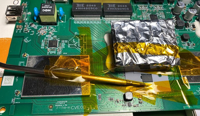
I also used a BBQ thermal probe to observe the board temperature and not to go very high. Honestly, this didn't help much and it was taking too much space so I removed it. To desolder the flash chip I put a lot of flux (flux is your friend and makes the solder flow), I started slowly, keeping the nozzle high to warm up the board and initially lowering it to the board to increase the temperature. Once the chip is removed, it was soldered (with the use of a hot air station) on the adaptor and the adaptor was plugged into the programmer.
In the next picture, you can see two things.
- how bad is my soldering on the pins on the adapter
- how my tweezers and inpatient hand damaged the casing of the chip (parts of the casing were chipped off)

Reading the flash chip data
The tool of choice for reading flash data is the SNANDer https://github.com/Droid-MAX/SNANDer. Unfortunately, I forgot to take screenshots from the tool. NOTE: You need to disable with -d the ECC checks otherwise you will get errors while reading the flash data.
Since the ECC checks are disabled and my soldering quality is poor I decided to dump 10 times the firmware, calculate the SHA256 hash and check for differences. Out of 10 dumps only 2 of them had different hash values and those two had the same bit flip. Therefore, with high confidence, we can assume that we had an error-free firmware dump.
Analyzing the dump
According to binwalk, the firmware dump seems be successful since there are meaningful data in the file. In order to understand whether the bootloader has to be analyzed, we need to identify if the actual root file system (most probably UBIFS) is encrypted.

Let’s extract the files from the firmware file and go for the UBI section. We can use the ubireader_display_info from the ubi_reader project https://github.com/jrspruitt/ubi_reader to read the characteristics. Unfortunately, something is wrong and the tool does not work.

Out Of Band (OOB) Data
We have to understand the NAND flash structure according to the flash chip specification. The NAND flash chip has a page area of 2048-bytes containing 4 segments of 512-bytes. After the 2048-byte area, there is an additional 64-byte spare area (four 16-byte segments for each page segment) containing the OOB data for the ECC correction codes, markers and metadata.
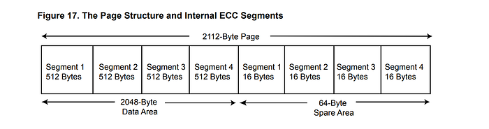
That means that our firmware dump contains additional metadata which break the firmware data sequence. I should have suspected that because the file was 132MB instead of 128MB. How the problem can be overcome? What if we remove this 64-byte section after each page? If there are errors in pages they might not be corrected since there is no ECC algorithm in place but let’s give it a shot. Before removing the OOB data let’s run a test first. In 010 Editor we can write a Template to highlight the OOB data.
typedef struct {
byte data[0x800];
} page_data;
typedef struct {
byte data[0x40] <bgcolor=0x0000ff>;
} spare_data;
while (!FEof()) {
page_data page;
spare_data spare;
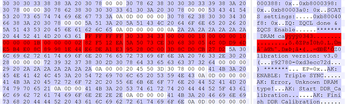
}If our theory is correct there might be a sequence of data like strings, that are separated by OOB. Apparently, there is. The word “calibration” is separated by the OOB data.
With few Python we can remove the OOB data.
buff = file_in.read()

for x in range (0,len(buff),0x800 + 0x40):
    file_out.write(buff[x:x+0x800])


file_in.close()
file_out.close()
The new file is indeed 128MB. If we use Binwalk again and run the ubireader_display_info again on the newly extracted UBI file we get no errors this time.

Finding the encryption algorithm
By using the ubireader_extract_images on the UBI file we are getting two pairs of UBIFS files. It is not clear why there are two files in the flash and most probably this will be concluded with further analysis.
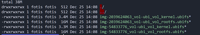
All files are SquashFS files. Let’s begin with the rootfs files since those contain the main binary and configuration files. By running unsquasfs immediately the process terminated due to errors. The ignore errors flag -ig is used to extract all files possible. However, both rootfs alternatives have errors and in both cases, some files were extracted and some other don’t.
As we discussed previously there is some uncertainty about the accuracy of the firmware (ECC errors or flash structure) so the engagement plan is to find the decryption algorithm of the firmware, in order to be able to decrypt the original firmware files which are published.
By looking at the extracted binaries the libfwutil.so caught our attention. Thankfully the binaries include symbols and make our life easier during the analysis.
Since the modem architecture is MIPS we are going to use Ghidra (the free version of IDA does not support MIPS). The function decrypt_fw is presented below. The first 0xA0 bytes of the firmware file are being read in a buffer. Then the offsets 0x60 and 0x20 of the buffer are used in FUN_00001e14 function.
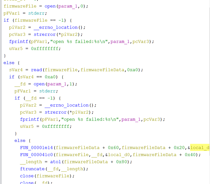
There are two important functions int the decryptor function. FUN_00001e14 where the encryption key is prepared and FUN_000041c0 where the AES265 algorithm is invoked.
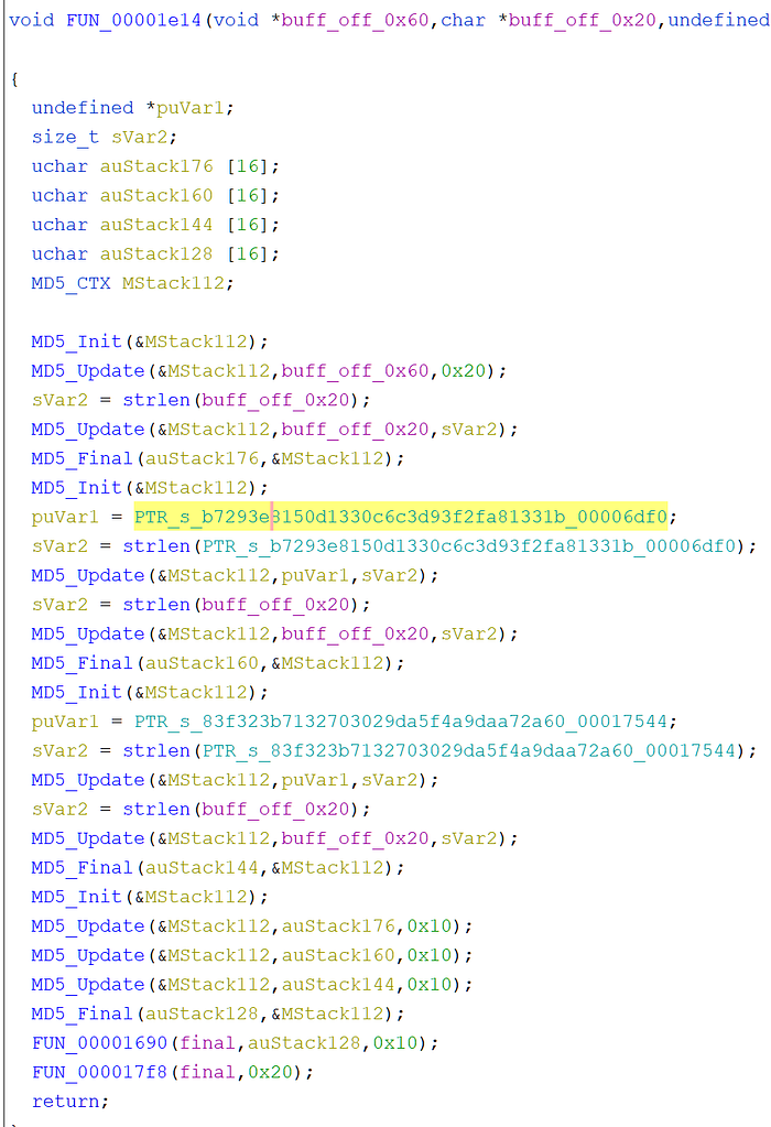
For FUN_00001e14 the high level algorithm is the following MD5(MD5(buffer+0x60),MD5(buffer+0x20),MD5(“83f323b7132703029da5f4a9daa72a60”),MD5(“b7293e8150d1330c6c3d93f2fa81331b_00006df0”))
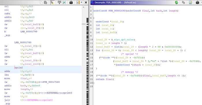
There are two additional functions that should be examined. FUN_00001690 and FUN_000017f8. In FUN_00001690 Ghidra does not do a great work on decompilation on MIPS architecture. Effectively the code converts the bytes to string hex.
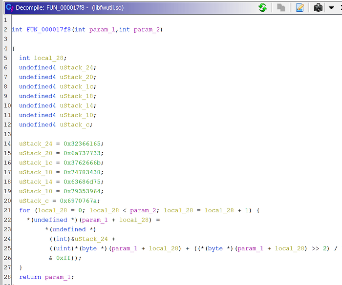
The other important function in the FUN_00001e14 is the FUN_000017f8. Again, not great work for Ghidra decompiler. The function implements a simple shift encryption algorithm based on string “26aejsw37bfktx48chmuy59dipvz”.
A cleaner view of the decompiled code can be seen below
int ii;
unsigned char key[28];
memcpy(key, "26aejsw37bfktx48chmuy59dipvz", sizeof(key));
for ( ii = 0; ii < 32; ++ii )
  *(unsigned char *)(md5_buffer + ii) = *(key + *(unsigned char *)(md5_buffer + ii) % 0x1C);
                                                                                                                                                                                                                                                                                                                                       127,1         Bot
To recap the AES256 key is generated by the following algorithm.
Derive_Key(MD5(MD5(buffer+0x60),MD5(buffer+0x20),MD5(“83f323b7132703029da5f4a9daa72a60”),MD5(“b7293e8150d1330c6c3d93f2fa81331b_00006df0”)),”26aejsw37bfktx48chmuy59dipvz”)
As a last step we have to take a look at FUN_000041c0 where the AES256 is invoked. The function is called with four arguments, the file handle for the firmware file, the file handle to write the decrypted firmware , the generated AES key and another offset in the firmware file (+0x40) which is passed as a parameter to AES_DecryptInit and therefore is used as the IV (take a look at the main decryptor image).

Conclusion
Now that we have a way to decrypt already published firmware files we do not have to worry about things like flash structure, ECC errors etc. as we are able to analyze the binaries with better accuracy and without extraction errors.
Some of the lessons learned:
- You cannot work with microscopic electronics without a microscope
- I managed to knock off components in the process and ultimately destroying the router
- When in doubt use binwalk, it always knows the way to extract files.
Since this is a new field for me you are welcome to provide comments and recommendations.
